Addressing the data challenges of modern electronic warfare and radar
StoryAugust 10, 2020
By Chris Miller, Keysight Technologies
Radar, electronic warfare (EW), and signals-intelligence (SIGINT) systems face new challenges from near-peer threats, requiring multigigahertz bandwidths, nanosecond latencies, and the ability to implement and field new EW techniques – all of them needed to deploy in seconds or minutes, not days or months. Reconfigurable FPGA-based signal processors, optical streaming interfaces based on the Optical Data Interface (ODI) standard, and low-overhead packet standards based on the VITA Radio Transport (VRT) specification, combine to deliver unprecedented performance and flexibility. These three new technologies converge to enable a new class of software-defined operational and measurement systems that are able to address these new challenges.
Whether the mission is to intercept and collect, analyze, or counter, the many wireless signals that crowd the electromagnetic spectrum (EMS) – a combination of new technology trends – is increasing the probability of earlier detection, assessment, and response. The EMS on an electronic battlefield is chaotic and complex; the ability to fully understand signal behavior in a real-world environment is crucial in the design and validation of the latest radar, electronic warfare (EW), and signals-intelligence (SIGINT) systems.
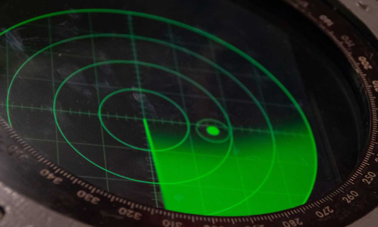
Let’s look at a simple example of the current deployed state (Figure 1). When an aircraft detects a radar signal, it goes to its EW system’s look-up table. Assuming it can identify the signal, the aircraft – or an adjacent one in this case – would correspondingly select an appropriate countermeasure signal to jam it. In development are EW systems that may be able to identify the class of a new, adaptive radar signal. These systems generate a countermeasure signal based on existing techniques that would allow some parameters to be adjusted, such as frequency or the pulse repetition interval (PRI). Unknown threats would still need to be recorded and analyzed in the lab.
[Figure 1 | Assuming it can identify the signal, the aircraft – or an adjacent one in this case – would correspondingly select an appropriate countermeasure signal to jam it. Image courtesy Keysight/NASA/USGS.]

Increasingly complex and diverse threats are driving the need for future EW systems to identify and neutralize these adaptive radar signals with cognitive countermeasures. As the EW threat environment continues to evolve, confidence and reliability in EW system validation and verification depends on improvements and modernization in the test and evaluation process.
There are several significant measurement challenges, however. First, the signals of interest are highly unpredictable, making them difficult to capture and recreate using traditional measurement methods. Fortunately, the latest digital hardware, processing engines, and interfaces enable the creation of RF [radio frequency] streaming solutions that can analyze, record, and play back signals for seconds, minutes, hours or even days. Another challenge is the resulting mountain of “Big Data”: Dealing with a glut of data calls for an optimized combination of measurement hardware and software, which can accelerate the data collection and make the analysis more manageable.
Applications such as radar target simulation and emulation require complex signals with frequency shift, delay, and channel effects. These signals have typically been generated and analyzed with digital signal processing engines or recorded to and played back from a deep-memory storage device such as a RAID [redundant array of independent disks]. One such block diagram of compatible instruments, including digitizer, arbitrary waveform generator (AWG), digital signal processor (DSP), and storage modules is shown in Figure 2.
[Figure 2 | Block diagram shows instruments used in radar target simulation and emulation.]

The digital processing engines in conventional radar and EW systems are often implemented with field-programmable gate array (FPGA)-based system-level architectures. These FPGA-centric systems implement digital RF memory (DRFM) and other EW techniques in firmware via VHDL and Verilog. They are sufficient for intercepting and analyzing known waveforms on their pulse descriptor word (PDW) list. Unfortunately, the engines can lack the dynamic flexibility needed when encountering new waveforms generated on the fly by near-peer adversaries.
Future EW systems will need to be built with new devices and technologies to counter these unknown threats from the software-defined digitally programmable adaptive radars that are emerging. By deploying a heterogeneous architecture based on a high-speed processing engine working in conjunction with a partially reconfigurable FPGA, the system can synthesize a mix of responses to quickly create the best defense against the new unknown threat.
Partial reconfiguration offers modification of FPGA
While FPGA technology offers on-site programming and reprogramming, partial reconfiguration (PR) takes this flexibility one step further. PR allows the modification of an operating FPGA design by loading a partial configuration file into reconfigurable regions of the FPGA. It does so without compromising the integrity of the applications running on those parts of the device that are not being reconfigured. This change of the FPGA image without rebooting has enabled dynamically reconfigurable instruments and could be deployed in operational systems as well.
PR is also useful in those situations in which an interface is required to persist while the functionality changes. For example, when a FPGA system is interfaced with a host computer via PCI Express (PCIe) a full reprogramming of the FPGA breaks the communication link. PR, in contrast, enables the link to be maintained by keeping the interface circuitry active while the accelerator portion undergoes reconfiguration.
High-speed communication links are essential between these processors plus storage and other devices to enable quick responses to the unknown signals and also to manage the enormous amount of data. The Optical Data Interface (ODI) is a new point-to-point interface standard for instrumentation and embedded systems. ODI breaks speed and distance barriers by using optical communication between devices over a pluggable optical fiber. With speeds as fast as 20 Gbytes/sec from a single optical port and as fast as 80 Gbytes/sec through port aggregation, ODI is designed to help address these challenging applications in high-speed data acquisition, data processing, and signal generation. By contrast, a PCIe Gen 3.0 by 8 lanes bus interface – commonly found between modules in a PXIe chassis – has a maximum data transfer rate below 8 Gbytes/sec.
The ODI standard specifies an MPO/MTP multifiber push-on optical connector, which may be placed anywhere on a device. ODI works with any product format, whether AXIe, PXI, LXI, VPX, or a traditional bench instrument design. It works equally well with embedded systems, such as those found in military or aerospace applications, as it does with instrumentation. Through the standardized ports, ODI enables high-speed communications between instruments, processors, storage, and embedded devices in various form-factor combinations when configuring hybrid systems and solutions. The ODI family of specifications is best described as three layers, with each of the layers working in concert to achieve a high degree of interoperability.
Layers at work
First, ODI-1 defines the physical layer, which is how bits and bytes get from one device to another. It describes a method of transporting packets, without defining what those packets are. This physical layer itself consists of two layers, an optical layer and a protocol layer. The optical layer consists of 850 nm VCSELs [radar target simulation and emulation lasers] and 24 lanes of multimode fiber optics, 12 in each direction. A device that transmits data is called a producer, and a device that receives data is a consumer, while there are two line rates, 12.5 Gb/sec and 14.1 Gb/sec. Devices that operate at the higher speed must operate at the lower speed as well, enabling upward compatibility. An ODI port is capable of over 160 Gb/sec per direction based on multiplying 12 lanes by 14.1 Gb/sec. (This rate is usually simplified as 20 GBytes/sec.)
The protocol layer is based on Interlaken, a chip-to-chip interconnect standard common in data centers, conceived by Cortina Systems and Cisco Systems. Interlaken is supported by the major FPGA suppliers and managed by the Interlaken Alliance. It can deliver packets of data over a large number of lanes at very high speeds. Interlaken doesn’t define the packets, only their boundaries as a block transfer; Interlaken manages the health and alignment of the 12 ODI lanes without interrupting the data transfer. It also enables flow control from a consumer to modulate the average speed from the producer.
Next, ODI-2 specifies the transport layer, which is where the packets transported by Interlaken are defined: ODI employs a standard packet definition, leveraged from the VITA 49 family of standards (The VITA organization is well-known for its VME and VPX standards, deployed in many embedded military and aerospace applications). VITA-49, known as the VITA Radio Transport (VRT) specification, defines common packet formats and protocols for software-defined radios. The VRT specifications have low overhead, are very general in nature, and are applicable well beyond radio communication.
Standard VRT packets are used for block transfers of data sent between devices, with consecutive VRT packets creating a “stream” of contiguous data. These VRT streams provide much useful information that can be extracted by software-defined SIGINT systems when attempting to locate, identify, and monitor a wide range of unknown signals. ODI-2 also uses VRT packets to aggregate ports and achieve proportionally higher data rates. For example, a four-port system quadruples the data bandwidth to 640 Gb/sec, or 80 Gbytes/sec.
Specifically, ODI has adopted VITA-49.2 for its packet definition. Embedded in the mandatory packet prologue are Stream ID, time stamps, and Class ID that identifies the data formats. VITA-49.2 time stamps are particularly important for radar systems, which must capture reflected pulses during precise intervals of time relative to the outgoing radar pulse.
Finally, ODI-2.1 defines certain data formats and context packets optimized for high-speed data streaming and processing. ODI-2.1 mandates 8-bit and 16-bit real and complex data transfers, along with specific methods for loading the data into the packet’s data payload. Context packets are used to indicate metadata about the data stream. Parameters may include the sample rate, reference level, bandwidth, or RF and IF reference frequencies. By adopting evolving standards that are being deployed in data centers and in embedded systems themselves, ODI expands its applicability from test and measurement to actual operational systems as well.
There are many challenges to the design and implementation of future cognitive systems. For one, the test system block diagram shown here in Figure 3 would be extremely valuable in developing and evaluating cognitive electronic attack algorithms. By creating an emulated environment and enabling hardware simulations of realistic conditions, such a system could validate that these algorithms will work when deployed in the field. This test system could be used for mission planning and training purposes as well.
[Figure 3 | Test system diagram: Scenarios, emulators, system under test.]

The realization of such a test system benefits from these same technology advances; employing them offers the opportunity to both tightly integrate the measurement and operational equipment and enable hardware-in-the-loop substitution.
In conclusion, the convergence of several technology advances – namely PR, ODI, and VRT – are enabling a new class of software-defined EW, radar, and SIGINT operational systems and companion measurement solutions with enhanced data-handling capabilities.

Chris Miller is currently a strategic planner in Keysight’s Technology Organization in Santa Rosa, California. Forty years ago, he joined Hewlett-Packard Laboratories in Palo Alto. The intervening time at HP, Agilent, and Keysight has been spent equally working in central technology organizations and as an R&D manager in signal analysis and lightwave product divisions.
Keysight
www.keysight.com