
Using high-performance SRAMs to increase performance in DSP-intensive applications
StoryJanuary 29, 2014

Suhail Zain
Cypress Semiconductor

Military applications such as radar, Software Defined Radio (SDR), smart munitions and target detection systems, Electronic Warfare (EW), aircraft imaging, and many more benefit from Digital Signal Processors (DSPs). DSPs accelerate performance using deterministic processing and have capabilities that include real-time signal processing, extremely high throughput, and reprogrammability. However, signal processing demands for radar, EW, and other programs continue to increase so DSP system users continue to search for innovation that will boost performance. That need is being answered by use of a combination of Quad Data Rate (QDR) Static Random Access Memory (SRAM) that - at a minimum - doubles the performance of more traditional Synchronous Dynamic Random Access Memory (SDRAM).
Digital signal processing encompasses techniques to manipulate signals after they have been converted into digital form as seen in radar processing. They are used for several functions in radar systems such as pulse compression, signal filtration, and pulse modulation. These components differ from general-purpose microprocessors in that they are designed for the types of fast mathematical calculations (multiplication and addition) most commonly used to design filters like FFT and Finite Impulse Response (FIR). Typically, FFT filters are used for domain conversion – time to frequency and vice versa – whereas FIR filters are used for signal separation and signal restoration.
There are two main hardware approaches for implementing DSPs: programmable DSP processors and FPGAs. In both approaches, the DSP architecture is optimized for DSP algorithms.
DSP processors
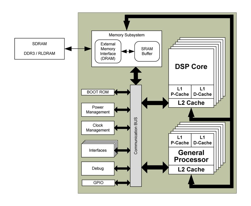
DSP processors like TI’s multicore DSP processor (shown in Figure 1) have specialized hardware to compute multiplication operations in one cycle. The instruction set of modern DSP processors enables programmers to specify several parallel operations in a single instruction, typically including one or more data fetches from memory in parallel with the main arithmetic operation. Furthermore, to significantly improve the DSP work per clock cycle, DSP architectures now include additional multipliers and adders for parallel execution, thus encoding parallel operations in a single instruction.
Figure 1: TI’s multicore DSP architecture.
(Click graphic to zoom by 1.8x)
|
|
FPGA-based DSPs
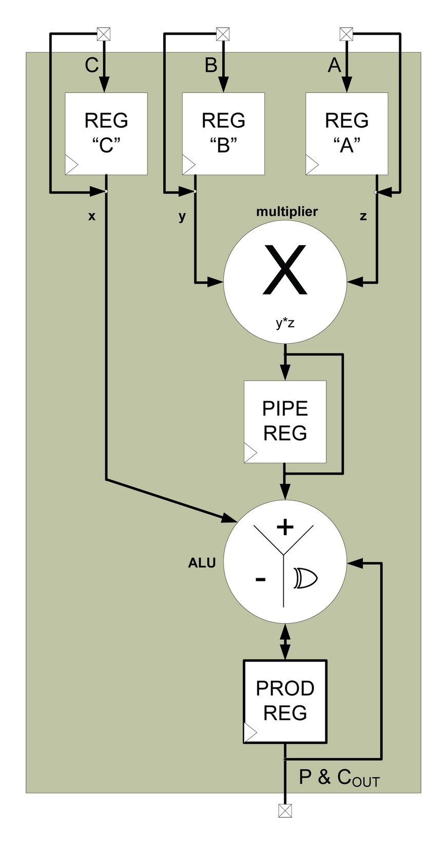
FPGAs like Xilinx’s Virtex, shown in Figure 2, have dedicated DSP blocks to efficiently implement DSP algorithms. Each DSP block includes dedicated hardware-based functions such as multiply, multiply/accumulate, add, shift, compare, bit-wise logic functions, and pattern detect. Wider mathematical functions can be realized by cascading multiple DSP blocks together.
Figure 2: Xilinx FPGA Virtex DSP architecture.
(Click graphic to zoom)
|
|
DSP memory requirements
Executing DSP functions every cycle requires the ability to fetch instructions and data from memory efficiently. This requirement means that high memory bandwidth is paramount to maintaining DSP performance. DSP processors, as well as FPGA DSP blocks, have developed internal cache memory architectures (L1/L2) to support multiple memory accesses per cycle. A Super Harvard Architecture is implemented where separate memory banks exist for instruction and data storage. With this arrangement, the processor can fetch both instructions and data operands in parallel every cycle. Moreover, memory accesses in DSP algorithms typically present a predictable pattern. For example, FIR filter coefficients are accessed sequentially and in a circular fashion. For deeper external storage, hardware-based External Memory Interfaces (EMIF) supporting various SDRAM memories (DDR2/3, RLDRAM) are typically employed. However, a new technique for external storage called Quad Data Rate (QDR) SRAM can improve DSP performance by a factor of two.
Improving DSP performance with QDR
QDR SRAM is a high-performance memory device optimized for high throughput. These memories have multiple independent data ports equipped with Double Data Rate (DDR) interfaces. Accesses to these data ports are concurrent and independent of each other. The address bus is common and runs at either single or double data rate, depending upon the configuration. The highest density product available today is 144 Mbit and can be configured as x18 or x36.
The architectural features of QDR-IV SRAMs work favorably with the digital signal processing flow in applications where high throughput, low latency, and random accesses are required.
Traditional (SDRAM) vs. new (QDR-IV) approach
Figure 3 illustrates the general setup of the test environment. FPGA-based DSP functionality is used where the maximum data throughput from different memory types is compared. Table 1 compares the major performance parameters between QDR-IV SRAM and DDR3 SDRAM memory technologies.
The table shows that QDR-IV provides more than twice the DDR3 SDRAM bandwidth running at the same frequency. Moreover, the dual independent ports of the QDR-IV SRAM facilitate a DSP’s real-time processing requirements on data where the output signal is produced at the same time as the input signal is being acquired. Using the QDR-IV, the bottleneck in transferring data to and from memory is alleviated.
Figure 3: Comparison of DDR3 SDRAM and QDR-IV SRAM test environments.
(Click graphic to zoom)
|
|
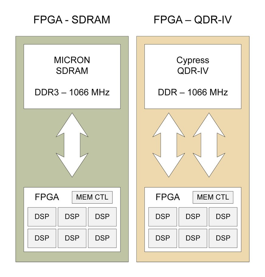
Table 1: QDR-IV and DDR3 SDRAM comparison.
(Click graphic to zoom by 1.9x)
|
|

SAR radar perspective
Synthetic Aperture Radar (SAR), which observes the Earth’s surface in high resolution, needs corner-turn memory access where the range direction and the azimuth direction are transposed for reconstruction processing. This operation is done for efficient FFT and IFFT (DSP) execution between range and azimuth compress processing. The architectural benefits of QDR SRAMs can improve SAR radar’s performance by allowing fast and uniform memory access times. Figure 4 shows the corner-turn problem with SAR image reconstruction.
Figure 4: Corner-turn with SAR image reconstruction.
(Click graphic to zoom by 1.9x)
|
|
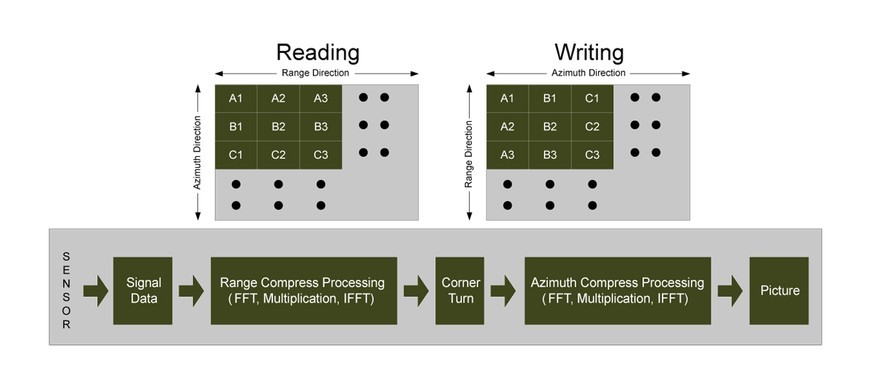
Using a conventional SDRAM memory, writing (as shown) of the SAR picture data ends up in a discontinuous address space, leading to a reduction in processor performance (in this case, estimated at roughly five times). Because QDR-IV’s independent ports for reading and writing enable concurrent operations and random memory access, the processing penalty is mitigated.
QDR SRAMs provide a beneficial performance alternative to conventional SDRAMs for off-chip data storage in DSP-based applications. Density limitation of QDR SRAMs can be mitigated by cascading multiple devices. This approach is ideal for applications where higher throughput with random access is required by enabling faster memory accesses for improved DSP performance.
Suhail Zain has been the director of new product development and strategic marketing for Aerospace & Defense at Cypress Semiconductor since 2010. He has more than 20 years experience defining, designing, and bringing to market state-of-the-art semiconductor products in reprogrammable technologies (FPGAs), high-speed memories (SRAMs), and trusted cryptographic solutions (TPMs). He earned both bachelor’s and master’s degrees in electrical engineering from the University of Southern California, with special emphasis on VLSI design. He holds more than 10 patents in design architecture.
Cypress Semiconductor 408-943-2600 www.cypress.com


