
Using DSP and RF circuit co-design to reduce risk and cost
StoryOctober 11, 2016

Murthy Upmaka
Keysight Technologies
In all areas of business, increased communication leads to more streamlined processes and greater potential for success. This is no less true in system design. Within large design organizations, baseband field programmable gate array (FPGA) and radio frequency (RF) signal processing communities have traditionally been separated both physically and by the resources available to them--with each group using very different techniques and tools. Today, however, many RF functions are moving into the algorithmic world and this is making communication between the two areas more crucial than ever.
Co-design, a process whereby all stakeholders actively participate in the design process, offers a solution. While organizations have certainly successfully designed electronic systems like wireless communication systems, smart phones, and space systems without co-design, its use offers not only the potential for reduced risk and cost, but accelerated time-to-market as well. It’s not surprising then, that the co-design of baseband algorithms and RF distributed circuits has emerged as a critical and important trend. For modern design organizations, it’s now more imperative than ever that they simulate both Digital Signal Processor (DSP) and RF circuits together at the system level using mixed signals.
Co-design: benefits and challenges
Co-design offers designers a number of important benefits such as when co-designing DSP and RF circuits, over design, inaccurate predictions, and difficulties in assembly can be prevented. In contrast, organizations that utilize disparate design flows with little to no communication and don’t co-validate along the way can anticipate added cost and complications. The algorithmic engineers have a hard time accounting for RF signal impairments in the signal processing, while those working on RF circuits aren’t able to clearly see how their systems are being used in the overall infrastructure.
Co-validation during the design process allows for some of these problems to be accurately accounted for, and lets organizations find the cheapest technique to solve a problem. Sometimes it’s cheaper to solve it with a better signal-processing algorithm. Other times it may be cheaper to buy a better RF amplifier. Knowing the best place to solve an issue and validating the solution before the final product is assembled is a benefit of an integrated, co-design approach, as is the ability to minimize over design and improve system performance for a given budget.
Despite these benefits, DSP and RF co-design is not without its challenges. DSP and RF circuits are simulated with different techniques. DSP is typically done in the numeric and time domain whereas RF circuits are designed using frequency-domain techniques. Converting between the two domains takes a long time and even when RF is changed into the time domain, many elements still exist in the frequency domain. You either have a very detailed RF model that is trusted completely, but need to simplify the signals, or arbitrary signals on the baseband side with an extremely simplified RF. Co-design bridges the gap, offering the right level of behavioral modeling on both sides.
While co-design of DSP and RF circuits can be used in many instances, it is particularly useful when designing phased array systems with adaptive beamforming where beam quality must be looked at in a system context. Additionally, it can be used for power amplifier linearization and envelope tracking, when changing the characteristics of the amplifier as a function of time. Co-design is also needed in end-to-end, wide bandwidth communications.
Co-design in Action: synthetic aperture radar
To better understand the concept of co-design, consider the design of an RF receiver with acceptable performance that will not render the algorithms ineffective, and in particular, a side-looking Synthetic Aperture Radar (SAR) on an airplane that covers an area on the ground. As the plane flies, its antenna beam sweeps the area. Linear frequency modulated radar pulses are continuously transmitted and return pulses are collected. Even if the ground is not visible with the naked eye from the plane due to clouds or fog, it is still visible to the radar due to the microwaves that penetrate these obstructions. From the returned pulses, an image is reconstructed. This reconstruction is enabled by signal processing algorithms. The returned signals are at microwave frequencies and, therefore, have to be properly down converted to the baseband before processing them. The RF receiver must perform this task without significantly degrading the signal quality.
The reflection from the target is constructed from a picture of the target in the form of JPG or GIF. The reflected signal intensity is proportional to the luminosity of the picture. This type of modeling of the SAR echo is very close to that happens in the field at the same time it is very fast to simulate.
Figure 1: From left to right, the impact of an increase in phase noise in the oscillator is shown. The amplifier is close to compression in the right image.
|
|

While evaluating the quality of the images produced, the RF amplifier, RF mixer, down converting local oscillator (LO), amplifier nonlinearity, LO phase noise, and mixer characteristics are all considered. In this case, the LO phase noise caused the RF receiver’s contrast to suffer slightly (Figure 1). Although difficult to pick up with the eye, the impact can be seen in numeric measurements.
On the other hand, a significant visible impact can be seen with the amplifier going into 1 dB compression. As it gets close to its compression point, a great deal of detail and sensitivity is lost and washed out.
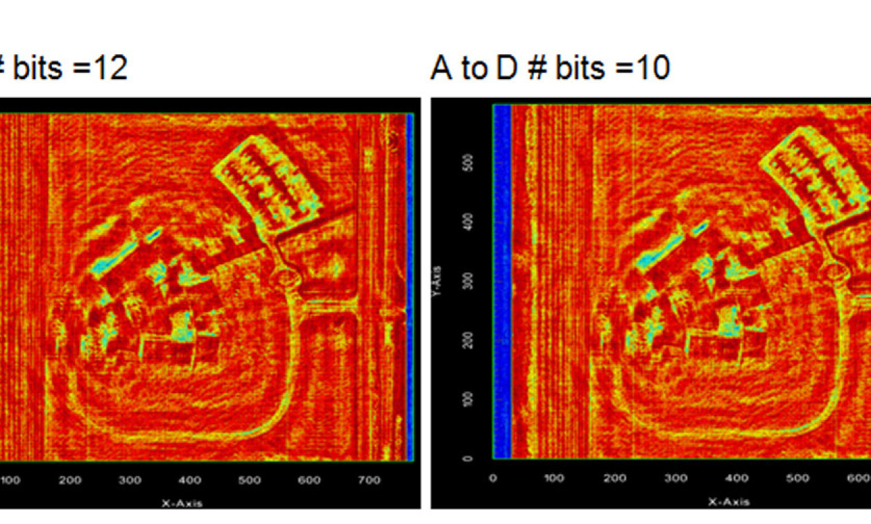
Figure 2: The change in image quality as A to D is changed from 14 to 6 bits can be observed from left to right
|
|

Loss of detail comes from other sources as well. For example, let’s examine an Analog to Digital Converter (ADC). When it is moved from 14-bit to 12-bit and then to 10-bit, banding starts and there is loss of detail (Figure 2). By the time 6-bits is reached, significant amounts of detail in the images are lost. At 6-bits, an Automatic Gain Control (AGC) may need to be added on the front end. Auto scaling can be performed to get it into the sweet spot of the ADC.
If some of these things are added together with low quantization levels, phase noise and saturation, it starts to not be useful. In this example, we have also added jitter. In addition to the ADC resolution, there is clock jitter that spatially limits the range resolution on the radar. Whole baseband signal processing is used to clean this up and make the signal. If the transmit and receive architecture is not designed to its best functionality, the ability to architect algorithms to overcome these issues may be lost. High fidelity is needed on both sides for the architecture and algorithms to work together.
By co-simulating both the RF and DSP worlds, the amplifier saturation has a relatively higher impact than the number of bits of the ADC. Further studies show that while performing this co-simulation, post-processing algorithms can be debugged and the optimal Fast Fourier Transform (FFT) size required for the pulse compression process derived.
In addition to co-design, co-simulation can be used to achieve faster, more accurate simulation. As an example, consider the co-simulation of an actual RF circuit used in the SAR that was designed using Keysight SystemVue Electronic System Level (ESL) software and Advanced Design System (ADS) software. The software and system-level simulator were connected together to create a simulated image that would be created by the SAR (Figure 3). By using the actual RF circuit, the semiconductor level models and board parasitic can be brought into the system-level simulation. The advantage of this approach is that amplifier nonlinearity, noise, input and output mismatch, AM-AM and AM-PM, and memory effects can all be captured in the simulation.
Figure 3: The top images show a SAR simulation with real circuit co-simulation performed using Keysight SystemVue and Advanced Design System (ADS) software. The bottom images show an SAR simulation with an X-parameter model.
|
|

This co-simulation is accurate; however, it significantly increases the simulation time. To reduce this time, the X-parameter model of the RF amplifier was captured and used in the system simulation (Figure 3). The X-parameter model preserved the accuracy and detail of the simulation, while significantly reducing the simulation time—in this case, by more than a factor of 10 compared to the circuit level co-simulation. Other advanced techniques like circuit envelope are available to further improve the co-design process.
By following this methodology, DSP-RF co-design can be accomplished and simulation times kept to a reasonable level. For modern design organizations, being able to co-validate these domains in one place, enables them to de-risk later aspects of a project, while also cross validating as they go. Ultimately, this allows for lower cost and faster time-to-market.
Dr. Murthy Upmaka, is an application engineer at Keysight Technologies. Upmaka’s work focuses on the Aerospace/Defense sector. Upmaka received a Ph.D in Physics from the Indian Institute of Technology, Madras.
http://www.keysight.com/find/eesof-systemvue-info


