
The benefits and challenges of using GaN technology in AESA radar systems
StoryOctober 11, 2019

Mario LaMarche
Mercury Systems
As the trend in the development of new radar systems shifts away from dish antennas and towards active electronically steered arrays (AESA), there is a growing need for high-power signal amplification distributed across the array. Whereas mechanically steered dish radars can use a single high-power amplifier to drive the antenna, AESA systems require multiple, compact power amplifiers. Achieving this level of high output power in a small space requires a solution with high power density and wide bandwidth – an ideal use case for gallium nitride (GaN) semiconductor technology. However, while GaN-based amplifiers offer substantial benefit, their implementation is not without challenge.
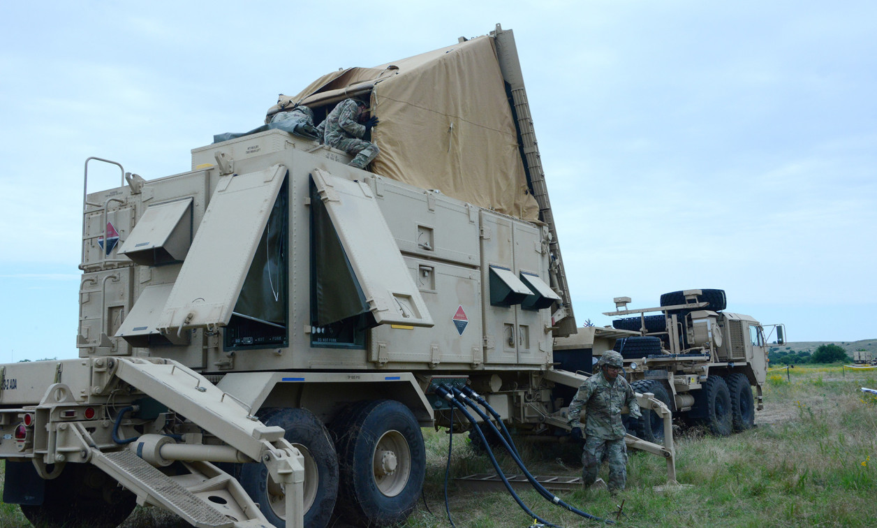
Unlike mechanically steered radar systems that determine the target’s location based on the physical orientation of the antenna, active electronically steered array (AESA) systems adjust the relative phase of each antenna element to steer the beam. This offers multiple advantages: For example, compared to a dish antenna it is much easier to mount a planar array to the body of an aircraft. Additionally, AESA radars offer more direct control over the direction of the beam and some even support multiple beams. This allows advanced radar capabilities to be deployed in new platforms while maximizing the ability to track difficult-to-detect threats. However, compared to a simple rotating dish antenna, implementing an AESA radar requires more advanced circuitry. In particular, each element of the AESA requires a transmit/receive (TR) module (Figure 1) that includes a phase shifter, switching circuity, a high-power amplifier for the transmit signal, and a low-noise amplification for the receive signal.
Figure 1 | Simplified block diagram of a TR module.
|
|

One of the most critical figures of merit for the AESA system is the range. In order for an object to be within the range of the radar, the reflected signal must be above the noise floor of the receiver, which we quantify by using the signal-to-noise ratio (SNR) calculation.
Most simply, optimizing the SNR of the TR module involves minimizing the noise figure of the receiver and maximizing the output power of the transmitter. While this sounds straightforward, it is complicated by the size constraints of the TR module and the need for high-frequency, wideband operation. Typically, the TR modules are arranged in a grid and placed behind the antenna elements. In order to fit all the TR modules, the height and width of each module is limited by the size of the individual antenna elements. As the operational frequency increases, the size of the antenna decreases. For example, at X-band the height and width of the TR module would be less than 2 cm.
Summarizing the design criteria: The TR module must be very small, have high output power, have a low noise figure, and operate at high frequencies. Clearly, maximizing the performance of TR modules is a significant challenge; however, it’s made easier through the use of GaN semiconductor technology.
GaN technology for TR modules
Gallium nitride, or GaN, is a semiconductor material with high breakdown voltage and high electron mobility. Similar to gallium arsenide (GaAs), the high electron mobility enables high frequency operation; unlike GaAs, however, the high breakdown voltage of GaN supports high electric field strength in the device. By operating at a higher voltage, GaN-based amplifiers are able to provide a much higher output power in a smaller space. (Figure 2.)
Figure 2 | Examples of various GaN-based amplifiers. Image: Mercury Systems.
|
|

Using GaN technology in the design of the TR module’s power amplifier maximizes the transmit output power while minimizing the physical size. In addition to shrinking the size of the amplifier die, the use of high-power GaN reduces the need to use many lower-power devices. Since the passive combining networks that are used to combine multiple die are large and introduce loss into the signal path, having fewer of them improves the power density in the TR module.
In addition to providing a high output power in a small space, the power amplifier in the TR module must be capable of operating at high frequencies. Depending on the specific applications, the radar may need to operate at X-band or even Ka-band. While there are other semiconductor materials that offer high power density, such as LDMOS, GaN is the best option for high-frequency operation. As an added benefit, GaN devices not only enable high-frequency operation, they also are an ideal choice for wide bandwidths.
In order to ensure effective operation, the AESA radar must include functionality to protect it against the effects of electronic attack. This is especially important as the technology to jam radars is becoming increasingly available. One method of achieving this resiliency is to operate the radar over a wide range of frequencies. Also, by modulating the frequency across a single pulse, known as chirp, the resolution of the radar can be improved. However, this requires the TR module to operate over a wider band of frequencies. Not only does GaN offer high power density, but when compared to GaAs, the higher bias voltage of GaN simplifies the process of designing a broadband impedance match. This enables a single GaN amplifier to operate over a wide bandwidth, enabling robust and multifunction AESA systems.
The higher bias voltage of GaN offers an additional benefit at the circuit level. Since power is the product of voltage and current, for a constant power, the higher bias voltage of GaN leads to lower current. When the current is reduced, the loss in the bias circuit is also reduced, which improves the efficiency of the amplifier.
GaN technology – while it can improve the performance of the output amplifier in the TR module – can also be used on the receive side. It’s a fact that maximizing the SNR requires both increasing the signal strength and decreasing the noise; when the receiver chain is examined, one source of noise is the protection limiter at the input to the low-noise amplifier since each dB of loss in the limiter equates to an additional dB of noise figure. By using GaN as the semiconductor material for the LNA, it is possible to design out the limiter since GaN can withstand higher input voltages without damage. This leads to a net improvement in the receiver’s noise figure, maximizing the SNR and the range of the radar system. Also, by removing the limiter from the design there is more space in the TR module for other circuitry.
Challenges of using GaN technology
While the benefits afforded by leveraging GaN technology in AESA TR modules are significant, the design and manufacturing processes are far more complex than simply removing a GaAs device and inserting a GaN device. In addition to developing techniques to manage the high levels of heat generated in such a small area, successfully using GaN technology requires an understanding of the many subtleties specific to this semiconductor material.
Managing heat and circuitry
The main benefit of GaN technology also leads to the main challenge: While high power density enables new applications, it also requires managing the heat generated by the devices. For example, consider a 30 W GaN amplifier die with a bias of 2.5 A at 28 V. This results in 40 W of power dissipation in a device not much larger than 10 mm square.
Managing this level of heat generation requires focused attention at each thermal interface, since even a small increase in thermal resistance results in a significant device temperature rise, degrading the long-term reliability. The first step in ensuring effective thermal management is optimizing the attachment of the GaN die to the baseplate. For example, using a gold-tin eutectic die attach process will provide much better thermal conductivity than silver epoxy. Additionally, the attachment process must be carefully controlled to prevent the formation of air voids under the die. To ensure the quality of the die attach, confocal scanning acoustic microscopy (C-SAM) can be used to check for voiding that would reduce the thermal conductivity and cause an unacceptable temperature increase in the device. (Figure 3 and Figure 4.)
Figure 3 | C-SAM image showing poor die attach due to excessive voiding.
|
|

Figure 4 | C-SAM image showing a successful die attach.
|
|

Moving away from the device, we also need to maximize the thermal conductivity between the baseplate and the housing body. For lower power applications we often see die installed on a Kovar baseplate due to its matched coefficient of thermal expansion (CTE). However, for high-power applications, a material such as copper molybdenum is likely a better choice as it offers lower thermal resistance.
In addition to the thermal challenges, designing an amplifier using GaN technology requires careful attention to the bias circuity. Whereas for GaAs devices, the gate current is negligible, for GaN the gate of the device draws significant current. Accommodating this current requires bias circuity with low series resistance and the capability of sourcing current. As an additional challenge, the pulsed nature of radar requires the bias circuity to support fast-switching gate current.
These two examples – thermal management and bias circuitry – highlight just a few of the challenges encountered when using GaN in amplifier design. Since every design is unique, the opportunities for technical issues are unlimited. In order to achieve the many benefits made possible by GaN, the design and manufacturing teams must have the experience and technical knowledge to overcome the challenges and come up with innovative solutions.
Mario LaMarche is product marketing manager for Mercury Systems. He previously worked at Teledyne Microwave Solutions and Samtec as product line manager and engineer. Mario holds MS and BS degrees in electrical engineering/RF and microwave design. Readers may reach Mario at [email protected].
Mercury Systems
www.mrcy.com


