
Releasing the full potential of FPGA-based designs
StoryDecember 22, 2009

Rob Evans
Altium Limited
For all the power and flexibility FPGAs bring to embedded designs, the additional development process injects new levels of complexity and constraint into the design workflow. Unifying the conventional hardware-FPGA-software design processes to make full use of FPGA reprogrammability is one way forward.
As FPGA technology barnstorms its way through the military electronics and systems and virtually all other sectors of the embedded electronics industry, applications exploiting the advantages of programmable logic are becoming a mainstay. Communications, airborne, and control systems in particular benefit from the design flexibility, field reconfiguration, and parallel processing capabilities of FPGAs, while the short design cycle and simpler verification process help to get applications into the field faster.
In spite of the FPGA’s pervasiveness, though, very few applications are truly harnessing the FPGA’s full potential for flexible design. This limitation results from the fact that FPGA development has simply been added to, or at best bolted on to, the traditional software-hardware workflow. This isolated FPGA development stage adds significant complexity to the overall design process.
To simplify the overall undertaking and restore design choices, the individual design processes – hardware design, software development, and program-mable hardware design – need to be brought together so they can be tackled as a single task. If this is implemented at a fundamental level where all the processes share a single pool of design data and common design environment, the dominant and unique advantage of FPGAs – reprogrammability – can be used to advance FPGA-based designs to the next level. Key to harnessing the full flexibility of FPGAs is an understanding of their evolution, design challenges, and what can be done to restore harmony among the three major FPGA-containing system design aspects: hardware, programmable hardware, and software.
FPGAs evolve from glue logic to SoCs
Upon entering the embedded market, FPGAs were first regarded as a convenient and efficient host for implementing large sections of “dumb” glue logic for which development need not involve or interact with other elements of the design process.
However, FPGA devices, and how they are used, have significantly evolved from the concept of convenient containers for mass digital logic. High-capacity FPGAs now host entire SoC designs, where core functional elements such as processors, memory, and high-speed data processing are implemented in the programmable space. In military embedded systems where the relatively low production runs struggle to justify a new ASIC start, FPGAs provided a viable, cost-effective path forward for harnessing the physical simplicity and reliability benefits of an SoC approach.
Compared to simple glue-logic designs, a major difference with SoC implementations is that software and hardware development are now fundamentally bound to, and dependent upon, the FPGA design. This is because FPGA devices and support peripherals are the center and core elements of the physical design, and the embedded application software is hosted within the FPGA space. As a result, any change in the FPGA domain will have a significant effect on the hardware and software domains.
Restrained innovation
Regardless of the interdependence between design domains, the conventional development process for an FPGA-based product design still reflects a traditional approach by regarding each part of the design (hardware, software, and now embedded hardware) as separate, disconnected tasks.
A change in one domain tends to lead to a disruptive, time consuming redesign in the others. This means that major decisions such as hardware-software partitioning must be made (and locked in) early in the design cycle – just as they were with traditional “non FPGA-based” embedded designs. In practice, physical hardware (FPGA devices and peripheral hardware) and then programmable hardware elements are locked down, in sequence, before meaningful software development can proceed.
Those initial decisions define the parameters and constraints for subsequent development processes, so the design options are increasingly limited through each sequential process. For example, the selected FPGA device (and hardware peripherals) will define a performance ceiling that includes identifying which embedded IP can be implemented. In turn, the embedded hardware design will define the functional capabilities available to the software. Or it could be as simple as the FPGA device only supporting soft processors supplied by that device vendor, which in turn defines the programming options available to the application software.
Additionally, pursuing concepts like fine tuning a design’s performance by moving software algorithms into embedded hardware, changing from an embedded to hardwired processor, or opting for a different FPGA device type will force a substantial redesign in all domains – hardware, programmable hardware, and software. For mil/aero systems development where hard deadlines are mandatory, the resulting design cycle disruption is untenable, so most engineers avoid tackling this type of design exploration at all costs. Yet invariably, high performance and design stability are also paramount, so investigating processor options and the potential benefits of soft-to-hard algorithm transfers is essential.
Restoring unity
As mentioned, simply adding the FPGA development process on to the existing design workflow constrains the ability to harness its full flexibility potential. In applications where the low NRE costs and rapid design are of particular advantage, the barriers imposed by conventional design processes are diluting those attributes. Yet this is just where FPGAs should be exploited to maximum effect.
The first step to restoring design choices and fully harnessing FPGAs is to bring the design processes – hardware design, software development, and programmable hardware design – into one sphere (Figure 1). By using a single design system and application that draw from a single data model of the entire design, the design domains can interact and respond when design changes are made in an individual domain. In practice, each domain is using a subset of the same design and component library data. As a result, design changes such as moving functions between software and hardware or exploring alternative devices are simplified, since a change can easily (or even automatically) be reflected through all the domains.
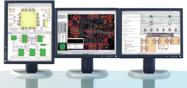
Figure 1: The full potential of FPGAs can be harnessed when embedded hardware development, physical hardware design, and software development all exist in a single, fundamentally connected design environment.
(Click graphic to zoom by 1.3x)
|
|
The design data and configuration files for the selected FPGA device, for example, are available to both the hardware and FPGA design domains, from the single pool of design data. If the FPGA device or its pin configuration is changed in the FPGA design space, that information is immediately available for implementation in the hardware design space. The action of exploring design options is more practical, while higher-level design functions like swapping pins between the hardware and FPGA design domains are simplified.
Exploiting reprogrammability
In this singular design environment, developers can finally start to fully harness the flexibility of FPGAs. Take a typical situation where the most practical placement of physical hardware components creates extremely complex FPGA-to-peripheral connectivity, in part due to high-density BGA packaging. One answer is to bring the parts of that routing complexity inside the FPGA itself, by making strategic board connectivity paths via the FPGA’s reassignable pins and internal routing.
Here, the FPGA’s pin reassignment and internal routing capabilities are used to solve a board routing challenge, potentially reducing the board area and number of layer requirements. This concept, again, relies on the existence of a hardware-software-FPGA development environment that is connected at the platform level, as this is required to support intelligent and automated pin-swapping between the hardware-FPGA domains.
This unified design approach also opens up the possibility of implementing global software systems that raise the abstraction of the design process – such as schematic or graphically based embedded design capture that is synchronized to both the hardware and software domains.
The natural extension of this design abstraction is to implement high-level embedded layers that effectively disconnect the soft elements of a design from the hardware on which it resides (Figure 2). These inserted layers “normalize” the interfaces between processors and hardware such as memory and peripherals, removing the need to deal with the low-level hardware complexity of I/O configurations and bus systems. Reconfiguring an FPGA design becomes a simpler, lower risk process, whether it’s rebirthing legacy designs, configuring different production modes, reusing established IP, or performing post-production updates.
Figure 2: Flexible SoC systems, including external “hard” components, can be plugged together using FPGA-based Wishbone bus architecture cores that act as versatile interfacing layers.
(Click graphic to zoom by 1.8x)
|
|

In practice, processors and peripherals can be supported by library-based FPGA cores based on the Wishbone bus architecture. The core abstracts a processor interface by effectively “wrapping” around the device, making it architecturally equivalent to other processors. It therefore allows a processor to be opportunistically changed without affecting the connected peripherals or forcing major redesign. Along with FPGA-based “soft” devices, the concept can be extended to include hybrid hard-core processors, external processors, and off-chip discrete peripherals and memory devices.
Next-generation FPGA design
The high-level unified embedded design approach outlined is made possible by capitalizing on the reprogrammable capability of the FPGA host. Any imposed layers and interfaces are automatically included in the FPGA’s fabric, along with the functional design itself, enabling the hardware design to be dynamically explored without fatally disrupting the other parts of the design.
Rob Evans is a technical editor at Altium Limited. He has more than 20 years of experience in the electronics design and publishing industry, and studied Electronic Engineering at RMIT in Melbourne, Australia. Rob can be contacted at rob.evans@altium.com.
Altium Limited 1-800-544-4186 www.altium.com


