
Radiation testing of CMOS devices required for space use
StorySeptember 11, 2017

Ross Bannatyne
VORAGO Technologies

Radiation testing of semiconductors is time-consuming and expensive. There are limited test facilities available and often a long waiting list to get "beam time." It is, however, an important part of product testing that is required for devices that will be used in high-radiation environments, such as space.
Rad-hard microcontrollers are processed using a hardening technique that immunizes the device from latch-up and enables full operation of the device while a total ionizing dose is accumulated up to 300 krad (Si). Rad-hard devices also should include an error detection and correction (EDAC) subsystem and scrub engine to address single-event upsets (SEUs) in memory. Dual-interlocked cell (DICE) latches are also implemented to prevent SEUs in logic.
Table 1: Expected performance of the VA10820
|
|

Total ionizing dose (TID) testing
When a CMOS device is present in a radiation environment, it may be subjected to a continual dose of particle radiation that causes degradation of performance, increase in leakage current, and ultimately failure of the device. Particle strikes cause electron-hole pairs to be produced in the silicon. Holes get trapped in oxide regions and as they accumulate over time, their presence creates leakage paths that result in increased current consumption and a shift in transistor Vt (threshold voltage) that causes device failure. The onset of the effects of TID can be observed through an increase of device current consumption.
TID testing on several rad-hard devices was performed at a facility at University of Massachusetts at Lowell. The high-dose rate gamma cave is an irradiation room having an equidimensional volume of 512 cubic feet. Several small ports penetrate one shielding wall to provide access for instrumentation cables. (Figure 1.) Irradiation and testing was performed in accordance with MIL-STD-883H Method 1019.8 Condition A.
Behind the metal plate shown in Figure 1, there is a Cobalt-60 source (immersed in water) that emits radiation to the devices under test (DUT).
Figure 1: TID testing in the gamma cave irradiation room at the University of Massachusetts, Lowell.
|
|
Four devices were mounted to a bias board so as to be exposed to radiation. All irradiations and tests were performed on the devices in static bias conditions with checkerboard pattern loaded in memory and nominal VDD. Prior to the TID test, all DUTs were tested using the production ATE test program and log files were generated for each DUT. During each TID test, irradiation was periodically halted so continued functionality of the parts could be verified and standby currents could be measured using the same test setup which maintained voltage bias on the parts during irradiation. The number of intermediate irradiation stops were kept to a minimum to reduce the annealing of TID-induced charge build-up in the device oxides. TID effects are annealed when radiation is not present – the device will return to its pre-irradiation state as the accumulation of positive charge in the oxide region naturally dissipates.
Following exposure, the devices underwent a full post-radiation electrical test. A sample of parts were placed on a 125 ºC, 24-hour bake then retested. All characteristics returned to pre-irradiation testing levels (without overshoot). The complete TID test process is shown in Figure 2.
The testing confirmed that an appropriately rad-hardened device will operate within specification at up to the datasheet parameter of 300 krad(Si).
Figure 2: TID test process
|
|

Heavy ion testing
The purpose of heavy ion testing was to confirm that the device meets the Soft Error Rate (SER) and latch-up immunity specifications detailed in Table 1. To confirm that the device under test meets SER specifications, multiple tests were conducted on with EDAC (rad-hard microcontroller with EDAC, scrub engine and DICE latches) and without EDAC (high temperature microcontroller without EDAC, scrub engine and DICE latches) to construct SEU Weibull plots for various modes of operation.
The Weibull plot parameters were used with the CREME96 modeling tool to determine SER performance under conditions of geosynchronous orbit solar minimum with 100 mils of aluminum shielding the conditions under which the device is specified). The linear energy transfer (LET) performance was observed directly by irradiating the devices using boron, argon, krypton, and xenon charged particles at various particle angles of incidence.
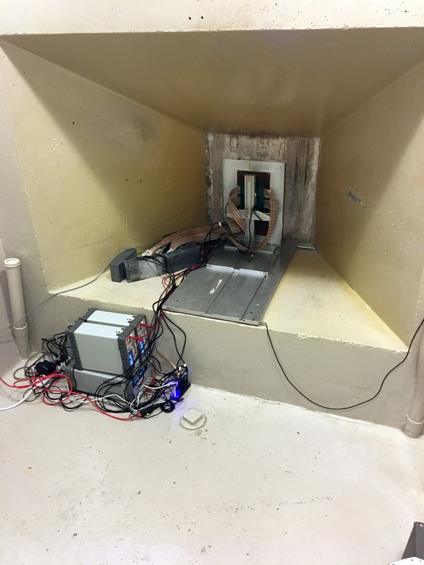
The heavy ion testing was performed at Lawrence Berkeley National Laboratory in Berkeley, California. The facility uses an 88-inch cyclotron to create charged particles and irradiate components that are located in a vacuum chamber in the irradiation room. (Figure 3.)
Figure 3: Irradiation room at Lawrence Berkeley National Laboratory.
|
|

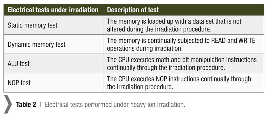
Two devices were mounted to the biased boards being exposed to radiation. The test procedure comprised of irradiating the Vorago devices VA10820 and VA10800 (control group) under four operating modes: static memory test, dynamic memory test, ALU test, and NOP test. These four tests were designed to examine radiation performance under different operating conditions and to help functionally isolate different parts of the circuits. These four tests are described in Table 2.
Table 2: Electrical tests performed under heavy ion irradiation.
|
|
Tests were conducted for several charged particle types: boron, argon, krypton, and xenon. In addition, the tests were repeated with the ion beam applied at different angles of incidence to the die (0º, 45º, 60º, 76º, and 80º). In all, there were two hundred unique tests conducted. In addition to this test procedure, additional high fluence tests (requiring high particle flux in the range of 2,000 to 3,000 particles/cm2/s) were performed with the objective to increase the probability of detecting single event latch-up, single event functional interrupt, and single event reset events. The complete heavy ion test process is shown in Figure 4.
Figure 4: Heavy ion test process
|
|

Bit upsets on memory can be observed by loading known patterns into memory and periodically comparing actual data to expected data. From this spatial and temporal data, bit upset data can be observed to determine how many logically adjacent bits can be upset by a single particle strike. The ion beam was adjusted to implement different angles of incidence (0º, 45º, 60º, 76º, 80º) to increase the likelihood of adjacent bit cells being upset. The worst-case condition that was observed during testing occurred with krypton particles at 76º angle of incidence.
This test resulted in four physically adjacent bit cells along the word line recording bit upsets. As the adjacent bits in a single EDAC byte of the device under test are physically separated by eight cells, this worst-case condition would not result in an uncorrectable multi-bit error (MBE) from a single particle strike as the upset bits are located in different bytes and are corrected by the EDAC and scrub engine subsystems (that can detect two-bit errors and correct one bit error per byte).
The SER is specified as <1e-15 errors per bit-day at geosynchronous solar min. with 100 mils of aluminum shielding and appropriate SCRUB rate. To determine how the CMOS operates under this specific orbital/solar condition, it is necessary to use the native condition Weibull parameters with the CREME96 simulator. The CREME96 simulation software is maintained by Vanderbilt University and enables the user to select the orbital environment that the device will be operating in. The operation of the EDAC and scrub engine must also be factored into the calculation. Increasing the frequency of the scrub engine reduces the average accumulated errors in the memory array, reducing the likelihood of uncorrectable multiple single bit errors in the same EDAC byte. The input data to CREME96 consisted of the native bit error Weibull fit parameters and the orbital/solar conditions were configured as geosynchronous solar min with 100 mils of aluminum shielding.
When the programmable scrub frequency is set to 500 Hz (one memory address scrubbed every 2 ms), the SER results in 2.65e-16 errors per bit-day, comfortably exceeding the product specification (1e-15 errors per bit-day at higher scrub rates).
No latch-up events on the devices were observed during any of the testing up to an Effective LET of 165 MeV-cm2/mg.
Terrestrial neutron testing
Terrestrial neutrons are a concern for operators of electronics that need to avoid equipment downtime due to neutron strikes in a terrestrial environment. Typical examples of such operators would be large server farms and telecommunications stations that use lots of electronic devices and memories.
Terrestrial neutron testing was performed using the neutron irradiation source at the Tri-University Meson Facility (TRIUMF) located at the University of British Columbia in Vancouver, British Columbia. The terrestrial neutron facility provides a neutron beam with a distribution of neutron energies comparable to those commonly found on the surface of the earth, but at much higher flux rates so accelerated terrestrial neutron testing can be performed.
The results of the testing are measured using a failures in time (FIT) rate. Terrestrial neutron FIT rate is the number of failures that would be expected due to terrestrial neutron-generated upsets in a specified amount of circuitry over 109 hours of device operation at sea level in New York City.
The rad-hardened devices demonstrated a lower FIT rate, although there was a low occurrence of errors so FIT rate is difficult to measure with precision. The system fault FIT rate is at a level one would expect purely from corrupted instructions in the memory code space, whereas the nonhardened system fault FIT rate was about two times what would be expected just from corrupted instructions in the memory code space.
The parts containing memory error detection and correction and other design-hardening techniques demonstrated terrestrial neutron FIT rates of < 1 FIT/device for device upsets and < 1 FIT/Mb for uncorrectable memory errors.
Rad-hard parts in use
VORAGO products are currently in operation on the International Space Station in the RHEME (Radiation Hardened Electronic Memory Experiment) project, a science study sponsored by NASA and created in conjunction with the United States Air Force Research Lab. The purpose of RHEME is to study the frequency and effect of high-energy particle strikes on CMOS memory chips in space.
Ross Bannatyne is director of marketing for VORAGO Technologies, based in Austin, Texas. He was educated at the University of Edinburgh and the University of Texas at Austin. Ross has published a college text called “Using Microprocessors and Microcomputers” and a book on automotive electronics called “Electronic Control Systems” (published by the Society of Automotive Engineers); he also holds patents in failsafe electronic systems and microcontroller development tools. Ross can be reached at [email protected].
Vorago Technologies
www.voragotech.com


