
Obsolescence management: Another perspective
StoryFebruary 10, 2009

Jack Bogdanski
White Electronic Designs Corporation
Obsolescence is most effectively managed when it?s considered from the beginning of product development at the design stage. Yet, solutions exist ? at every level ? that can save a project, an application, or even a program from redesign forced by obsolete components. Key factors include the lack of visibility in increasingly complex technology development, lengthy and costly redesign cycles, and fragmented communication channels.
A major consideration for both components and an overall systems design approach is obsolescence. Having a component or the materials it’s made from go obsolete can have a dramatic impact on the long-term viability of a product life cycle. The component and its materials are critical in product design and development for the defense and aerospace industries where communications, aircraft, navigation, guidance, and radar systems require long-term reliability and upgradability.
Obsolescence management techniques can be categorized as either production engineering-based techniques (that attempt to control an existing situation) or design-based techniques (that attempt to minimize the initial problem). While there are no quick or easy solutions, using production- and design-based obsolescence management techniques can minimize the problems faced on long life-cycle programs. In particular, it’s essential to anticipate and mitigate: the lack of visibility in increasingly complex technology development, lengthy and costly redesign cycles, and fragmented communication channels.
Visibility is important
Defense manufacturers are very small fish in the large sea of the semiconductor world. The defense market is less than 0.5 percent of the semiconductor industry and gains little attention or influence over the semiconductor suppliers (see Table 1, courtesy of the DoD and Databeans).
Table 1
(Click graphic to zoom by 1.9x)
|
|

The defense budget grows just 1 to 2 percent per year and will likely never be significant enough to change its level of visibility in comparison to the commercial industry. Although the COTS initiative was put in place to save money, it often adds expense to a program because of the natural procurement focus on unit price; many solutions end up tied to commodity-driven parts with rapidly changing design cycles that drive fast obsolescence cycles. Worse, IC suppliers rarely provide change notifications to defense contractors or their suppliers; this creates unforeseen obsolescence management challenges when a problem finally ripples through to a military program.
Certain military programs, such as weapons systems, can be more affected than other programs by this lack of visibility. Obsolescence can severely impact weapons systems’ supportability and life-cycle costs. It’s a fact that it can cost from millions to tens of millions of dollars to replace, redesign, or requalify a product simply because a $30 part went obsolete.
When a major Korean semiconductor manufacturer announced the end-of-life for their Rev. C SRAM product and the beginning of production for their Rev. D component, it was an abrupt transition. There was no lifetime buy to be had, and that particular SRAM had been highly used in RAD-tolerant applications. The satellite market, poised to take Rev C, a $6 RAD-tolerant device, instead was suddenly forced to use a $6,000 RAD-hardened component. Clearly there was minimal or no visibility provided to the vendor that was forced to fund a 1,000x price increase.
Navigating by silicon road map is a production engineering-based approach to manage this obsolescence issue. Large semiconductor manufacturers release road maps that extend 12 to 24 months. These road maps detail the products that are going EOL and the new products that are scheduled for delivery. These road maps can be reviewed for new products that can fill the role of the ones that are going EOL, allowing modifications to certain systems or subsystems with minimal disruption.
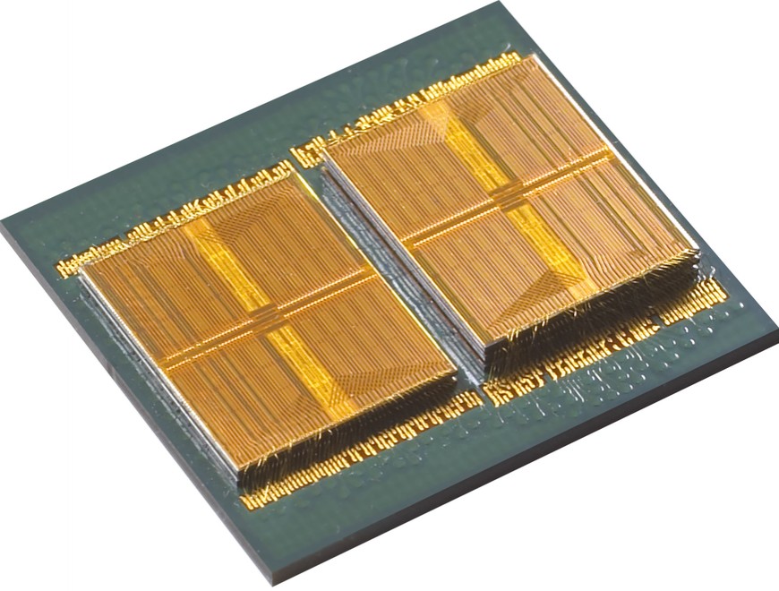
For example, consider a 32M x 72 DDR2 DRAM FBGA component specified in a design (Figure 1). With road maps, one can design in the additional address lines and control signals in order to prepare the way for the next two generations of replacement products. In addition, the road maps can often provide proper design floor planning for any additionally needed package space for those upgrades. Even in cases where the die information is not available that far in advance, a team with established memory experience can provide very strong suggestions based on past trends. There’s a huge cost savings in the long run. The entire design doesn’t need to be requalified or respun, and often the qualification takes place at the component block level. With advance notice of the next generation, one can plan ahead for upcoming changes.
Figure 1
(Click graphic to zoom by 1.9x)
|
|
Redesign cycles can be minimized
Microelectronics obsolescence is most often the result of basic economics: When it is no longer economical to produce a certain product, the semiconductor manufacturer stops producing it. Design-based techniques can alleviate obsolescence management challenges. It’s a matter of changing the perspective to save the design. For example, an established functional schematic with diodes and transistors in a discrete solution experiences an unanticipated EOL issue with one of its components. Oftentimes that portion of a system design can be segregated as a functional block and can be supported by bringing the entire block onto an FPGA. By replacing old technology with new technology, the change frees up board space and also often utilizes programmable devices to achieve a longer product life. It will look like a different board, but from an electrical perspective, the overall functional block is the same to the application. One can change or consolidate the components into a new functional block without changing the form, fit, or function of the overall system, and essentially keep the design.
Die Redistribution Layer (DRL) can also be implemented to allow the die pads that fit that die to move into a package it was never designed to support. A DRL allows solder paste bumping of legacy die that can transform off-chip connections from chip scale to board scale, providing a design-based solution that can support the form, fit, and function of a previous requirement and save the system from a costly redesign.
With die shrinks, in many cases, the electrical parameters change and thus force a redesign. Military microelectronics manufacturers might do a lot of die banking. For instance, White Electronic Designs banks up to 30 percent of its die inventory – especially flash and SRAM – so the company can complete a program, though repairs and maintenance might still be a problem. Both customer-specific and generic die are banked. If a flash product is going away and it’s used on 20 different programs, 100,000 parts might be banked just to have on-hand.
A large military OEM requested that a 5 V flash that goes into a custom module in a GPS guidance system be die-banked for them so that they would not be forced to use the next-generation die, which has a lower operating voltage that is not supplied on the board. If they did not make this request, the OEM would have to requalify at the board level, the box level, and then the system level, creating extra expense and delaying implementation.
Clear communications channels are essential
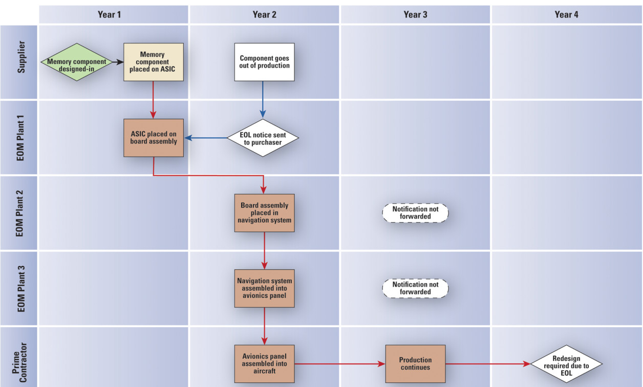
There’s an ongoing problem with EOL notification that permeates the industry and requires attention from the highest levels. As an example, a component is built for an OEM application and delivered to one of their plants, where it’s built into an assembly. Then they send it on to another plant to be assimilated into another assembly. From there, it might go on to another one or two locations for further integration and assembly.
However, the component that was designed-in for a two-year production order goes out of production in the second year. So an EOL notice is sent to the procurement office contact who bought the part. Maybe the contact is still there, maybe not, and the notice never goes on to the other four facilities in which the product was assembled. There’s a lack of incentive on the part of either the supplier or the purchaser to notify others down the line. This example is illustrated in Figure 2, where it results in a redesign.
Figure 2
(Click graphic to zoom by 1.9x)
|
|

Critical military programs are scheduled so far in advance that by the time they’re built, parts designed-in might already be at the end of their supported product life. For example, the Eurofighter was initially designed in the 1980s, but production didn’t occur until the late 1990s. The program has technology refresh schedules for most components, every year or two, with major refresh schedules at each manufacturing lot. The F-35 is also constantly being upgraded. Most of the systems in the F-35 Joint Strike Fighter (JSF) were designed seven years ago and just went into production. It will already need upgrades in 2009 and 2010 – only a year after it entered service! With lengthy military design cycles and no clear communications channel, an OEM doesn’t have much to rely on to get critical EOL information.
Both commercial and government websites provide military semiconductor device information and services to help alleviate technological obsolescence management pressures. TACTech Inc.’s databases and libraries contain the nomenclature and general description for more than 133,000 individual military semiconductor devices. TACTech’s military library generally includes all standard microcircuits and discrete devices with catalog specifications. TACTech software provides a description and general specifications of each microcircuit and discrete device in the TACTech library, thereby allowing the user to identify functionally interchangeable devices from various manufacturers and to upgrade and rank devices according to packaging, quality levels, projected production life cycle, and availability based on changes in technology and supply sources.
The Defense MicroElectronics Activity (DMEA) also offers obsolescence management services through the continual active monitoring of a system’s parts to stay ahead of the obsolescence curve and plan ahead for mitigation activities through production engineering-based obsolescence management techniques. The DMEA’s Advanced Reconfigurable Manufacturing for Semiconductors (ARMS) facility can produce any quantity, small or large, of microelectronic devices. Managers of weapons systems can use ARMS as a single solution or as part of a comprehensive supportability solution. If a large number of components is approaching obsolescence, a program manager can use ARMS to develop these microelectronic replacement parts as a temporary measure while redesigning and fabricating an entirely new system or subsystem.
The offerings from TACTech and the DMEA do not solve all the underlying obsolescence issues, however, because these efforts are still fragmented. Because fragmented communications channels impact the entire defense industry, the time might be right for the government to engage in more proactive obsolescence management activities using both a production- and design-based obsolescence management approach. There could be a government-controlled centralized website where all semiconductor manufacturers provide notice of EOLs. Military contractors could have master data systems with BOMs linked to this site so that they have instant notice at any time of a part going EOL. Vendors would post their notices to one centralized location for all military contractors to view. When the military contractors were tied into the database, they could elect to be automatically notified for all the programs with an EOL part. It would be managed electronically and handled by those most affected. A centralized obsolescence notification system could save the United States millions of dollars in just plain resource hours.
Identifying effective and manageable solutions
Technology creators in the defense industry should combine production engineering- and design-based obsolescence management techniques into an integrated approach to effectively and efficiently meet the challenges associated with obsolescence management: extended product life cycles, preplanned product improvements, modernization, technology refresh, and operational system development. These designers could use production engineering-based techniques for the first development phase, finding EOL buys, while at the same time employing design-based techniques, then planning for technology insertion system enhancements to be integrated later in the product life cycle. This is a good compromise for many applications, providing the benefits of the two techniques while minimizing the problems associated with each of them.
Custom semiconductor packaging that leverages commercially available die technology also combines the best of both techniques. Leveraging volume-driven silicon provides flexibility by opening up effective alternatives for handling obsolescence concerns. For example, a design might call for four plastic COTS discretes in packages with lead-free terminations that are prone to “tin whisker” growth. Instead, four die can be put in one package with lead-based terminations, thus saving cost by reducing the cost of failure. It would also conserve board space while providing a product in a package that has been proven mechanically reliable according to military requirements.
Also, it’s wise to use the most recent part available. The cost difference, even if significant at the time of development, will surely be minimal or even advantageous by the time of the program’s production release. Push for the highest density. Then look for the upgrade path – that’s critical.
While obsolescence is an issue for all of us in this industry, solutions do exist, and by working together with improved visibility, engineering creativity, and relevant and actionable communication programs, together we can minimize its impact.
Jack Bogdanski is Director of Strategic Development, Defense & Aerospace, at White Electronic Designs. He has 30 years’ experience in the electronics packaging industry, including multichip modules, memory, and microprocessor devices, flip chip assembly, bump metallurgies, alternative alloys, and flexible circuits and laminates. He holds a BSEE and an MBA from Arizona State University. He can be contacted at [email protected].
Mark Downey is Director of Strategic Development, High-Performance Computing at White Electronic Designs. He has 16 years’ experience in the electronics industry in the areas of high-speed memory bus architecture, electrical design and simulation, thermal management, multichip module packaging, and process development. He co-holds a U.S. patent in the area of Dense Memory Module Packaging. Mark also holds a BSEE from the University of Massachusetts at Lowell. He can be contacted at [email protected].
White Electronic Designs
602-437-1520
www.whiteedc.com


