From Wall Street to the military: Advances in FPGA switching technology and software-to-hardware development tools facilitate wire-speed data transmission
StoryJune 01, 2012

Brian Durwood
Impulse Accelerated
Douglas Gourlay
Arista Networks

Reversing the historical trend of the U.S. military being the first to develop key technologies that fan out to the rest of society ? such as the Internet, radar, and lasers - Wall Street is now funding ultra-low-latency data transmission technologies facilitated by advanced FPGA switching techniques and unconventional software-to-hardware development tools.
For federal agencies, the military, and other segments of modern society, there is an increasing world of data that would ideally be processed at full resolution and at wire speed. Wire speed means full data rate and as close to zero latency as possible such that there is no lag, no buffer, and no writing to memory. Full resolution means that there has been no compromise on the data stream sampling. This is significant, as some systems achieve wire speed only by reducing the sampling rate.
Meanwhile, the backbone of the Internet today is increasingly Ethernet network switches and routers. Recently there have been generational advancements in switch technology, where a programmable processing element is added very close to the ports and on the same mainboard as the rest of the switch hardware. The processing element is an FPGA, which comes off the shelf with more than 5 million logic elements. FPGAs are best suited to this location because of their parallel processing capability and higher, more flexible input and output options as compared to an ASIC. This provides the ability to instantiate a semicustom multicore computer at the edge of the wire. FPGAs in this use are ultra-low latency, programmable, and very flexible; however, software developers must learn a few new tricks to efficiently move their C algorithms to an FPGA.
Technology “trickle up”?
In an odd reversal of historical U.S. military “trickle down” by which government technology investments brought industry the Internet, radar, and the laser, development of this ultra-fast FPGA switch technology is being funded by Wall Street where winners and losers are separated by nanoseconds. What Wall Street discovered was that acceleration by parallelism trumps acceleration by clock speed. So as microprocessors approach limits of single-core clock speeds, efforts are shifting to “multicore” and extending parallelism. Basically for nonsequential logic, each process that can be run in parallel increases system throughput fairly linearly. Throughput often doubles with the first few parallelizations.
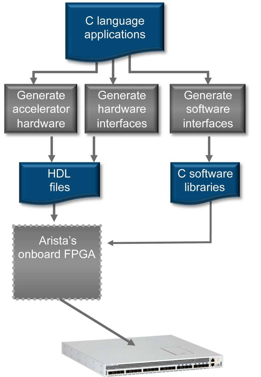
The latency and throughput effort shifting towards parallelism has FPGAs coming into prominence as processors in military technologies and elsewhere. Even at FPGAs’ slower clock speeds (and cooler operation), their extreme advantage in I/O and the ability to provide multiple cores enable FPGAs to be deployed at lower latency than traditional microprocessor implementations. FPGAs have been clocked at 2 microseconds in round-trip, wire-to-wire transactions. The optional soft-core processors allow code to be partitioned, some to compile into FPGA hardware and some to run “natively” in the onboard processor core (Figure 1). Or multiple parallel processes can run “natively” on multiple cores in the programmable switch.
Figure 1: C language files are partitioned to run in switch-integrated FPGA hardware or “natively” in C on the optional soft-core processor in the programmable switch.
(Click graphic to zoom)
|
|
The trend
To create seamless network insertion with a programmable dataplane represents an advance. The legacy option to use an appliance and somehow glue it to a switch or router has evolved into a fully capable switching and routing node that handles access control, QoS, and forwarding logic coupled with an inline programmable subsystem that is directly integrated with the forwarding plane, resulting in 24 1/10GbE wirespeed ports in a compact 1RU chassis. The integrated subsystem is optimal to run latency-sensitive and mission-critical applications directly in the switch, improving performance and determinism while reducing overall latency and costs. A built-in SSD is included for advanced logging, data captures, and supporting embedded applications. The application switch subsystem includes an Altera Stratix V FPGA with 160 Gbps of wire-speed performance and 6.2 million gates.
How to work with this technology
Programming many gates in a hardware description language is time consuming and increasingly an uncommon skill. This has instigated a shift toward compiling software to hardware. This shift has software teams scrambling to understand the differences. Tell a software developer that memory is no longer free and that access to I/O requires hardware drivers, and their eyes glaze over. Explain how the final compile to hardware can take hours and they begin to worry. Even with that, estimates are that there have been about 5,000 successful software-to-hardware projects completed in the past decade. The key is to stay as much as possible in a common High Level Language (HLL) such as C and to use tools to optimize the algorithm for operation on FPGA hardware.
Popular high-performance uses of this methodology include:
a. Inserting analytic modules or filters in-line: This is useful for algorithms for monitoring agencies like filters for unstructured data, FFTs, pass/no pass filters, and intrusion detection – anything that needs to operate at wire speed.
b. In security, inserting encryptors/decryptors with some type of activity flag is a common use as is wire-speed intrusion detection and lawful intercept.
c. On Wall Street, it’s mostly data-based routing – stock symbols, SMS message content, compliance, and automated trading. The federal agency equivalent could be looking for specific data with zero or low latency (that is, at wire speed).
d. DSP functions such as signals intelligence and radar systems targeting technologies are also common.
e. Useful in deep buffers for long “fat” network satellite problems.
Typically design begins “device independent,” where a C file is wrapped and brought into the tool flow. Analytics provide instrumentation to illustrate where there are opportunities for increasing parallelism or for how the stage delay propagates from specific lines of C. In the case of deep packet inspection, the focus of this design phase is typically the filters, wherein the designer iteratively refactors C to maximize parallelism (Figure 2).
Figure 2: The design flow starts with standard software development tools, analyzes flow for blockages, then provides detailed stage delay depiction and analysis.
(Click graphic to zoom)
|
|

Developers begin with untimed C, validating that the algorithm to run in hardware is equivalent to the original microprocessor-oriented version. The process from there is iteratively unrolling loops, increasing parallelism and reducing clock cycles. The Impulse C software-to-hardware compiler accepts untimed C. “Untimed” refers to C code that does not include additional information related to register boundaries, clocks, and reset logic. Impulse C automatically parallelizes C code, and there is no need to express such parallelism at the level of individual statements or blocks of code. To do this, it analyzes C code, finds interdependencies, and collapses multiple C statements into single instruction stages representing a single clock cycle. This automated creation of parallel hardware can be controlled by the programmer (for size/speed trade-offs) using compiler pragmas (Figure 3).
Figure 3: Parallelism involves unrolling a software process into multiple parallel hardware processes.
(Click graphic to zoom by 1.9x)
|
|

Some of the early C-to-FPGA tools relied on PAR and other embedded hardware specific statements, which limited their ANSI C compatibility. Newer, more flexible tools defer the hardware-specific elements to as late in the design flow as possible to retain full ANSI C compatibility. First-level verification is done within Visual Studio or the equivalent. The output is synthesizable VHDL (or Verilog) with three uses:
- It exports to the FPGA maker’s place-and-route tool for compilation to gates.
- It exports (optionally) to powerful simulators such as Mentor’s ModelSim or Aldec’s Active-HDL for cycle accurate simulation. Remember, the design involves more than 5 million gates, so verification at each step is critical.
- Some key VHDL routines are segregated at this stage for hand optimization. The trick is to keep as much as possible in C, facilitating migration to next year’s FPGA, and only hand-tweak the modules with the highest performance potential.
Hardware dependencies are inserted in a layer called a Platform Support Package (PSP). Here, board manufacturers create links to the hardware functions that can be accessed by C-level commands. This is sometimes referred to as the “plumbing.” PSPs are typically provided as source for the development teams that need to modify them.
Acquiring known-good code is also increasingly common in rapidly deploying image processing, packet inspection, and other processing-heavy tasks. Sometimes the code modules are for drivers and other noncritical elements, but increasingly highly optimized portions such as TCP/IP offload engines and encryptors can be acquired as Intellectual Property (IP). Acquiring known-good code cuts development time and improves performance. All of it remains ANSI C compatible, and even the new software-to-hardware functions make common sense to most software developers (Figure 4).
Figure 4: Language elements familiar to C coders are added in to accommodate hardware yet maintain ANSI C compatibility.
(Click graphic to zoom by 1.9x)
|
|

New architecture = new opportunities for speed
Putting the FPGA into a programmable switch, as close to the wire as possible, creates a new trend in integrated platforms, which is rapidly gaining the interest of both Wall Street and federal agencies and soon the military. Working with the platform is a little different from classic microprocessor-based development, but still accessible to both hardware and software engineers.
Douglas Gourlay is a Vice President at Arista Networks. which products are used throughout the intelligence and defense communities for mission-critical network infrastructure in mission-oriented systems. Prior to Arista, he led the product management and marketing functions for Cisco Systems’ data center technology group and has more than 25 patents in networking technologies. He can be contacted at doug@aristanetworks.com.
Brian Durwood is a cofounder of Impulse Accelerated Technologies which products are used by 8 of the top 10 government contractors and many federal agencies and branches of the Department of Defense. He was part of the original Data I/O ABEL team and then a Vice President at a Tektronix company, where he led a group creating high-frequency analog and digital multichip modules. He can be contacted at brian.durwood@ImpulseAccelerated.com.
Arista Networks 408-547-5500 www.aristanetworks.com
Impulse Accelerated Technologies 425-605-9543 www.ImpulseAccelerated.com